Why EMI Shielding Matters in Modern Electronics
Electromagnetic interference (EMI) is one of the most persistent challenges in electronics manufacturing. As devices become smaller, faster, and more densely packed, the risk of signal degradation from radiated and conducted emissions grows exponentially. For SMT assembly lines across Southeast Asia, where high-volume production of smartphones, IoT devices, and automotive modules is the norm, EMI compliance is not optional — it is a regulatory requirement and a competitive differentiator.
Nickel-plated SMT components play a critical role in this landscape. The nickel layer provides a robust, conductive barrier that reflects electromagnetic waves while resisting the oxidation and corrosion that can degrade shielding performance over time. Understanding how to specify and apply these components correctly can mean the difference between passing FCC/CE certification on the first attempt and costly redesign cycles.
How Nickel Plating Provides EMI Shielding
EMI shielding works through two primary mechanisms: reflection and absorption. Nickel-plated surfaces excel at both. The high electrical conductivity of nickel creates an impedance mismatch that reflects incident electromagnetic waves, while the magnetic properties of the material absorb energy across a wide frequency spectrum.
In SMT applications, nickel plating is typically applied as an underlayer between the copper substrate and a gold or tin finish. The nickel layer serves a dual purpose: it prevents copper diffusion into the final finish (which would compromise solderability) and provides the primary EMI attenuation layer. Typical nickel plating thicknesses range from 3 to 8 microns for shielding applications, with thicker layers offering better low-frequency attenuation.
Shielding Effectiveness by Frequency Range
The performance of nickel-plated shielding components varies with frequency:
- 30 MHz – 1 GHz: Excellent attenuation (40–80 dB). Nickel’s magnetic permeability makes it particularly effective at blocking low-frequency magnetic fields that aluminum or copper alone would transmit.
- 1 GHz – 6 GHz: Very good attenuation (30–60 dB). At these frequencies, reflection from the conductive surface dominates. Surface finish quality becomes critical — micro-roughness increases effective shielding area.
- Above 6 GHz: Good attenuation (20–40 dB). Skin effect concentrates current at the surface, making the plating thickness less important than surface conductivity and seam integrity.
Design Considerations for EMI Shield Components
When selecting nickel-plated SMT components for EMI shielding, several factors require attention:
1. Plating Thickness and Uniformity
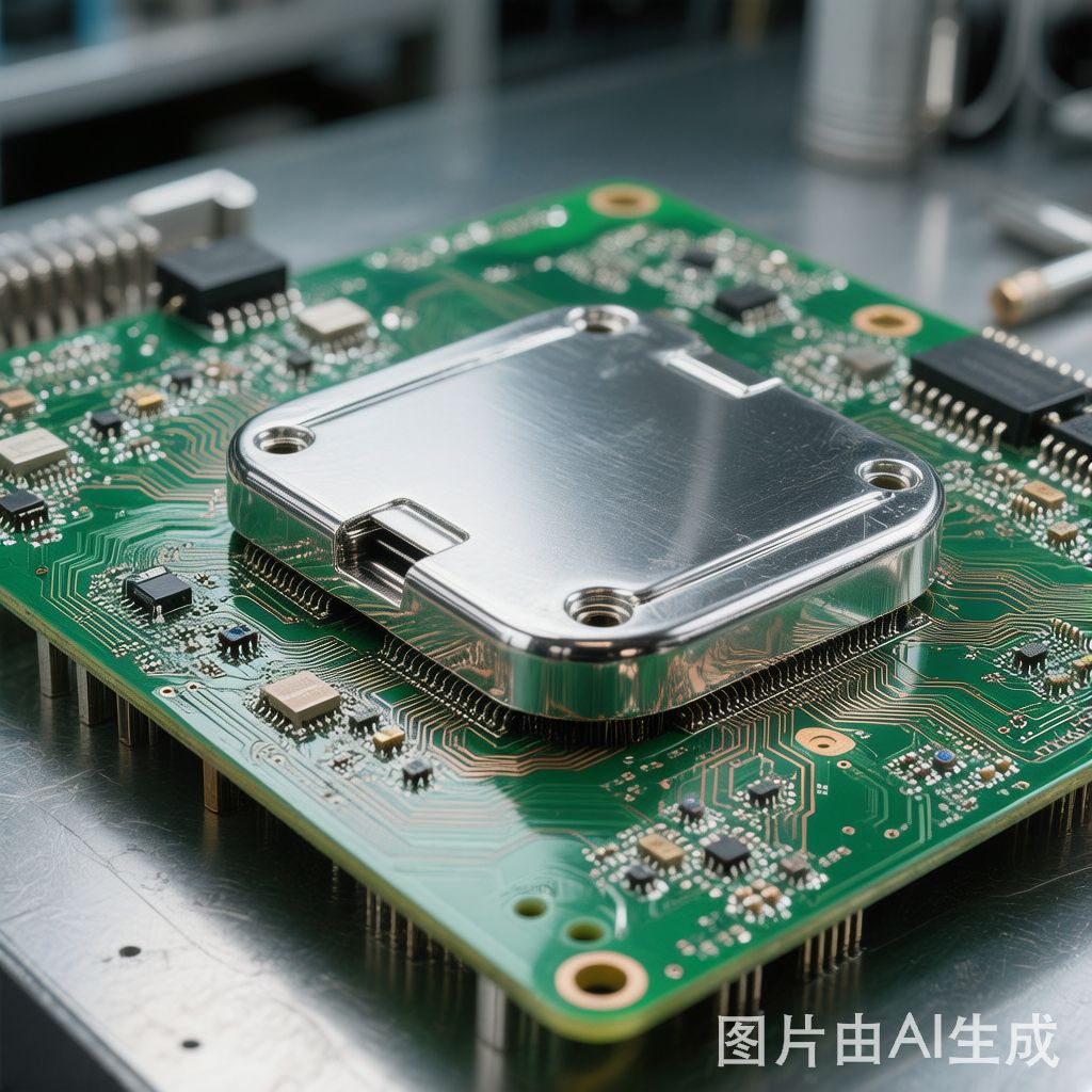
For wave soldered assemblies, a minimum nickel thickness of 5 microns is recommended to withstand the thermal cycle without exposing copper. Electroless nickel (EN) plating provides the most uniform coverage on complex geometries, making it the preferred choice for shielding cans and covers with embossed features.
2. Grounding and Contact Resistance
EMI shielding is only as effective as its ground co
ection. The contact resistance between the shielding component and the PCB ground plane should be below 10 milliohms for optimal performance. Nickel-plated spring contacts or conductive gaskets compressed against ground pads provide reliable low-impedance paths. For SMT shield cans, the standoff height and pad geometry must be designed to ensure full contact after reflow.
3. Ventilation and Aperture Design
Shielding components often need ventilation apertures for thermal management or component access. The maximum aperture dimension should not exceed one-twentieth of the wavelength of the highest frequency to be shielded. For shielding up to 6 GHz, this means keeping all apertures below 2.5 mm. Arrays of small holes perform better than a few large openings at equivalent open area.
Manufacturing Best Practices
On the SMT production line, several practices help maximize shielding performance:
- Stencil design: Ensure sufficient solder paste volume on ground pads. Insufficient solder leads to gaps between the shield can and the PCB, creating leakage paths.
- Reflow profile: Use a profile that fully melts the solder paste without causing the nickel plating to dewet. Excessive peak temperatures above 260°C can cause intermetallic growth at the nickel-solder interface.
- AOI inspection: Check for bridging between ground pads and signal pads on shielding can footprints. A single bridge can short the shield and create a radiating ante
a rather than a shield.
- In-line EMI testing: Integrate pre-compliance EMI measurements at the end of the SMT line to catch shielding failures before boards move to system assembly.
Cost Optimization for High-Volume Production
For contract manufacturers in Vietnam, Thailand, and Malaysia producing millions of units a
ually, the cost of shielding components matters. Nickel plating adds approximately 8–15% to the component cost compared to bare copper, but this is far less expensive than adding secondary shielding measures (conductive coatings, shield tapes) at the system level. Standardizing on a few nickel-plated shield can sizes across product families can further reduce tooling and inventory costs.
Conclusion
Nickel-plated SMT components offer a proven, manufacturable approach to EMI shielding that balances performance, reliability, and cost. By paying attention to plating thickness, grounding design, aperture geometry, and production process controls, electronics manufacturers can achieve consistent shielding performance that meets international standards while keeping production costs competitive.


