The Challenge of 5G RF Density
Modern 5G sub-6 GHz and mmWave modules pack power amplifiers, low-noise amplifiers, filters, switches, and transceivers into extremely small areas. At these frequencies, unwanted electromagnetic coupling between circuits can degrade receiver sensitivity, increase noise figure, and cause regulatory emissions failures. Board-level EMI shielding using metal cavities is one of the most effective ways to isolate sensitive blocks.
Unlike simple sheet-metal covers, effective shielding cavities require careful design of the fence, cover, apertures, and grounding strategy. This article explains the practical rules that RF engineers follow when laying out shielded modules.
Shielding Effectiveness Fundamentals
Material and Thickness
Board-level shields are usually made from tin-plated steel, nickel-silver, or phosphor bronze with thicknesses of 0.15–0.25 mm. The shielding effectiveness depends on reflection, absorption, and multiple internal reflections. At mmWave frequencies above 24 GHz, skin depth becomes very small, so even thin metal layers can provide high attenuation provided seams and apertures are controlled.
Seam and Contact Resistance
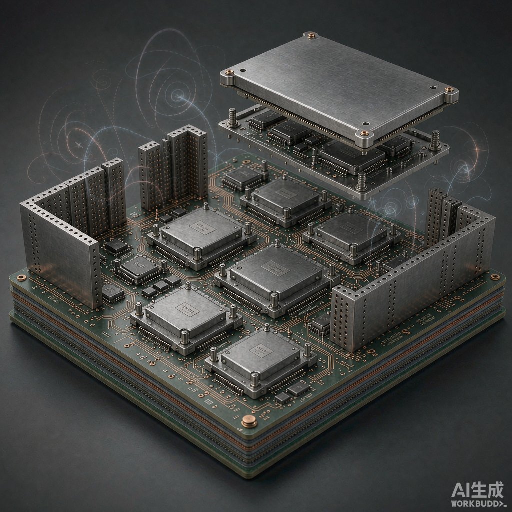
The weakest point in most shields is the seam between the cover and the fence. A continuous soldered fence provides the best isolation. For removable covers, spring fingers or dimple contacts must maintain low impedance across the full temperature range. A target contact resistance below 1 mΩ per centimeter of seam is a practical starting point.
Cavity Layout Strategies
Single vs. Multi-Cavity Shields
When multiple circuits share one large cavity, energy can bounce between them. Multi-cavity shields divide the board into separate compartments for transmitter, receiver, VCO, and digital control sections. The partition walls should extend from the PCB ground plane to the cover, forming a continuous Faraday cage around each block.
Aperture Placement and Size
Every ventilation hole, tuning slot, or co
ector cutout acts as an aperture. The rule of thumb is to keep the longest aperture dimension below λ/20 at the highest frequency of concern. For 28 GHz mmWave, that means holes smaller than 0.5 mm. Honeycomb vents or arrays of small holes preserve airflow while limiting EMI leakage.
Grounding and PCB Integration
The shield fence must co
ect to a low-inductance ground plane through numerous vias. A via fence with 0.3 mm diameter vias spaced 0.8–1.0 mm apart is common. Traces should never cross under a shield fence unless they are buried deep in an internal layer and well isolated. Keep high-speed digital lines away from RF cavities to minimize common-mode coupling.
Manufacturing and Assembly Considerations
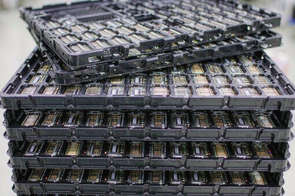
Two-piece shields (fence + cover) allow rework and tuning during prototype phases. Once the design is validated, a one-piece soldered shield can be used for production. Pick-and-place compatibility, cover retention clips, and thermal expansion matching should be evaluated early to avoid assembly issues.
Conclusion
Board-level EMI shielding cavities are essential for reliable 5G RF and mmWave modules. By controlling materials, seams, apertures, and grounding, engineers can suppress coupling, protect receiver sensitivity, and meet stringent emissions requirements in compact RF systems.