Why Gold Coating Matters for EMI Shielding Components
Electromagnetic interference (EMI) shielding components—whether stamped metal cans, conductive gaskets, or plated plastic housings—rely on consistent, low-resistance electrical pathways to divert or absorb unwanted electromagnetic energy. The surface finish applied to these components plays an outsized role in determining shielding effectiveness over the product lifetime. Among all metallic coatings, gold stands apart due to its unique combination of properties: it does not oxidize or tarnish in any atmosphere, it maintains stable contact resistance across decades of service, and it offers exceptional corrosion resistance even in aggressive environments such as salt spray, sulfur-bearing atmospheres, or high-humidity tropical climates.
For EMI shielding applications, gold coating is typically applied as a thin functional layer (0.05–1.5 µm) over a nickel or copper underlayer. The gold prevents oxidation of the underlayer at cut edges, contact points, and gasket-sealing interfaces where galvanic corrosion or fretting degradation would otherwise compromise shielding performance. While the material cost of gold is significant, the quantities used in thin functional coatings are modest, and the reliability benefits often justify the expense in high-reliability telecommunications, aerospace, and medical electronics.
The two dominant industrial processes for depositing gold onto EMI shielding components are electroplating (also called electrolytic plating) and physical vapor deposition (PVD), specifically sputtering and evaporation. Each process offers distinct advantages and limitations in terms of coating uniformity, adhesion, porosity, substrate compatibility, throughput, and cost. This article provides a detailed technical comparison to guide process selection for specific EMI shielding applications.
Electroplating: The Established Industrial Standard
Electroplating deposits gold from an electrolyte bath containing gold salts (typically potassium gold cyanide, KAu(CN)₂) onto a conductive substrate co
ected as the cathode in an electrochemical cell. The process is mature, widely available from job shops worldwide, and capable of depositing gold layers from 0.05 µm to 5.0 µm or thicker with good control. For EMI shielding components, typical specifications call for 0.25–1.0 µm of hard gold (alloyed with cobalt or nickel for wear resistance) or soft gold (99.9% purity for solderability and wire bonding) over a 2.5–5.0 µm nickel strike.
The electroplating process offers several compelling advantages. First, it achieves conformal coating on complex geometries including deep-drawn shielding cans with internal ribs, bent finger-stock contacts, and threaded fasteners. The electrolyte flows into recesses and cavities, ensuring complete coverage provided that racking and agitation are properly engineered. Second, plating baths can be scaled to handle very large production volumes—reel-to-reel plating of stamped strip components achieves speeds of 1–10 meters per minute, making electroplating highly cost-effective for high-volume consumer electronics. Third, the equipment capital cost is moderate; a standard barrel or rack plating line represents an investment of $50,000–$300,000 depending on capacity and automation level.
However, electroplating also carries limitations that must be considered. The coating is not perfectly uniform; current density varies with workpiece geometry, leading to thicker deposits on edges and thi
er coverage in recessed areas. This “dog-boning” effect can be mitigated with shielding and auxiliary anodes but never fully eliminated. Porosity is another concern: electroplated gold layers thi
er than 0.5 µm typically contain pinholes that expose the nickel underlayer to corrosive environments. For applications requiring maximum corrosion protection, minimum gold thicknesses of 0.75–1.0 µm are specified, increasing material cost. Finally, the cyanide-based electrolytes used in most gold plating operations require rigorous waste treatment and workplace safety protocols, adding operational complexity and environmental compliance cost.
Physical Vapor Deposition: Precision for Demanding Applications
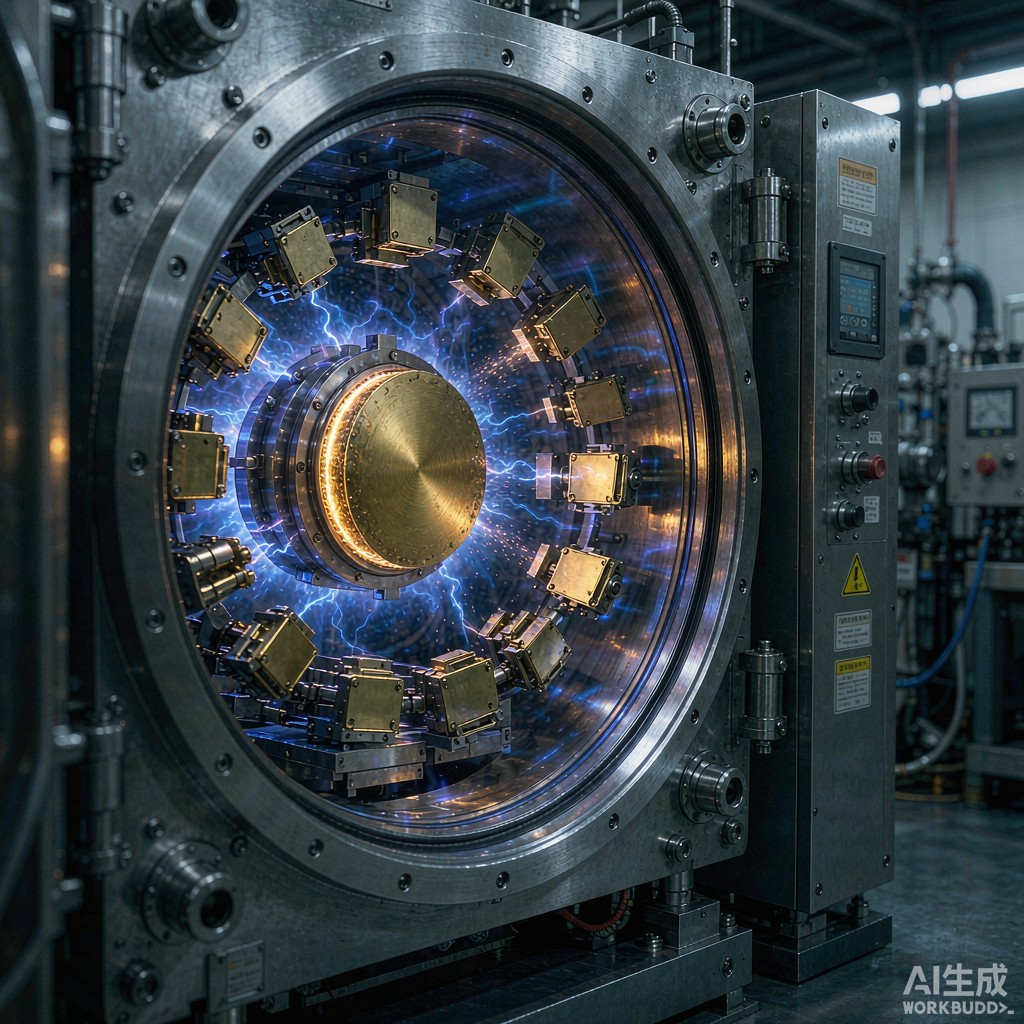
Physical vapor deposition encompasses two primary gold deposition techniques relevant to EMI shielding: thermal evaporation and magnetron sputtering. In both processes, gold is transferred from a solid source to the substrate in a high-vacuum chamber (10⁻⁴ to 10⁻⁷ mbar) without involving a liquid electrolyte. Thermal evaporation heats a gold crucible or filament to its vaporization temperature (approximately 2,970 °C at 10⁻⁶ mbar), creating a directional stream of gold atoms that condenses on the substrate surface. Sputtering uses a plasma discharge to bombard a gold target with inert gas ions (typically argon), ejecting gold atoms that deposit onto the substrate with higher energy and better adhesion than evaporated films.
PVD gold coatings are characterized by exceptional purity—often 99.99% or higher—and extremely fine grain structure. The coating thickness can be controlled with nanometer precision using quartz crystal microbalance monitors, making PVD ideal for applications where gold consumption must be minimized without sacrificing functional performance. For EMI shielding, PVD gold layers of 0.1–0.3 µm on a nickel underlayer can achieve effective corrosion protection and stable contact resistance, provided the coating is dense and pore-free.
The advantages of PVD are most pronounced in specialized applications. Because deposition occurs in a vacuum chamber, there are no wet chemistry hazards, no rinse water to treat, and no risk of hydrogen embrittlement in high-strength steel substrates. The process can deposit gold onto non-conductive substrates such as plastics and ceramics without requiring an initial electroless conductive layer, enabling direct metallization of molded EMI shielding housings. PVD coatings exhibit superior adhesion to properly prepared substrates because the high-energy sputtered atoms penetrate surface oxide layers and create metallurgical bonding at the interface.
The limitations of PVD are primarily economic and geometric. Vacuum chambers have finite capacity, and the batch-processing nature of PVD limits throughput compared to continuous reel-to-reel electroplating. A production PVD system represents a capital investment of $500,000–$2,000,000, an order of magnitude higher than electroplating. Coating uniformity on complex three-dimensional geometries is challenging because the directional nature of vapor flux creates shadowing in deep recesses and behind protrusions. Rotating fixtures and planetary drives improve coverage but add cycle time and mechanical complexity.
Performance Comparison for EMI Shielding
Shielding Effectiveness
Both electroplated and PVD gold coatings provide excellent electrical conductivity (~45 × 10⁶ S/m for bulk gold) and therefore contribute negligibly to surface impedance at frequencies below 10 GHz. The dominant factor in shielding effectiveness is not the gold layer itself but the integrity of the underlying conductive substrate—typically nickel-plated steel, phosphor bronze, or aluminum—and the quality of gasket-sealing interfaces. For this reason, shielding effectiveness measurements per IEEE 299 or MIL-STD-285 rarely show statistically significant differences between electroplated and PVD gold finishes of equivalent thickness on identical substrates.
Corrosion Resistance and Porosity
This is where process differences become meaningful. PVD sputtered gold films, due to their dense columnar microstructure and high adhesion, typically exhibit lower porosity than electroplated layers of equivalent thickness. A 0.2 µm PVD gold film on nickel can outperform a 0.5 µm electroplated film in salt spray testing per ASTM B117, because the electroplated layer contains more through-thickness pinholes that provide electrolytic pathways to the underlayer. For marine, aerospace, and chemical processing environments where corrosion resistance is paramount, PVD offers genuine performance advantages that can justify its higher process cost.
Wear and Contact Durability
EMI shielding components that experience repeated mating and unmating—such as slide-on shielding cans, removable cover plates, and RF co
ector shells—require wear-resistant gold finishes. Hard gold electroplates, alloyed with 0.1–0.5% cobalt or nickel, achieve Knoop hardness of 130–200 HK25 and withstand thousands of insertion cycles. Pure PVD gold is softer (60–80 HK25) and wears more rapidly under mechanical rubbing. Some PVD practitioners address this by depositing gold-titanium or gold-nickel alloy films, but these are less common and more difficult to control than established hard gold electroplating formulations. For high-wear applications, electroplated hard gold remains the default choice.
Substrate Compatibility
Electroplating requires an electrically conductive surface. Non-conductive substrates such as ABS, polycarbonate, or glass-reinforced nylon must first receive an electroless nickel or copper layer before gold electroplating can proceed. PVD can deposit gold directly onto any clean, vacuum-compatible surface, eliminating the electroless step and its associated process control requirements. This makes PVD particularly attractive for lightweight molded EMI shielding housings where adding an electroless layer introduces weight, cost, and potential adhesion failure points.
Cost Analysis and Volume Considerations
For low-to-medium volumes (1,000–100,000 units a
ually), PVD is generally more expensive per part due to batch-processing overhead and high capital depreciation. However, because PVD can apply thi
er, denser gold layers with equivalent or better functional performance, the material cost savings can partially offset the process premium. At very high volumes (>1 million units a
ually), electroplating’s continuous processing and higher deposition rates typically win on total cost.
A simplified cost model for a stamped shielding can (50 mm × 50 mm × 10 mm) with 0.5 µm gold over 3.0 µm nickel illustrates the trade-off:
- Electroplating: Process cost $0.08–0.15 per part; gold material cost $0.12–0.25 per part (depending on spot price); total $0.20–0.40 per part.
- PVD sputtering: Process cost $0.25–0.50 per part; gold material cost $0.05–0.10 per part (thi
er, denser coating); total $0.30–0.60 per part.
For premium applications where reliability is critical, the 30–50% cost premium of PVD is often acceptable. For consumer electronics where every cent matters, electroplating remains the dominant process.
Conclusion
The choice between electroplating and PVD for gold coating on EMI shielding components depends on a nuanced evaluation of performance requirements, substrate material, production volume, and total cost of ownership. Electroplating offers proven scalability, conformal coverage on complex geometries, and wear-resistant hard gold options for high-cycle applications. PVD delivers superior coating purity, lower porosity, direct deposition onto non-conductive substrates, and precise thickness control for material-cost optimization. For the majority of high-volume consumer electronics, electroplated gold continues to provide the best balance of performance and cost. For aerospace, medical, marine, and premium telecommunications equipment where failure is not an option, PVD gold coatings offer reliability advantages that justify the process investment.